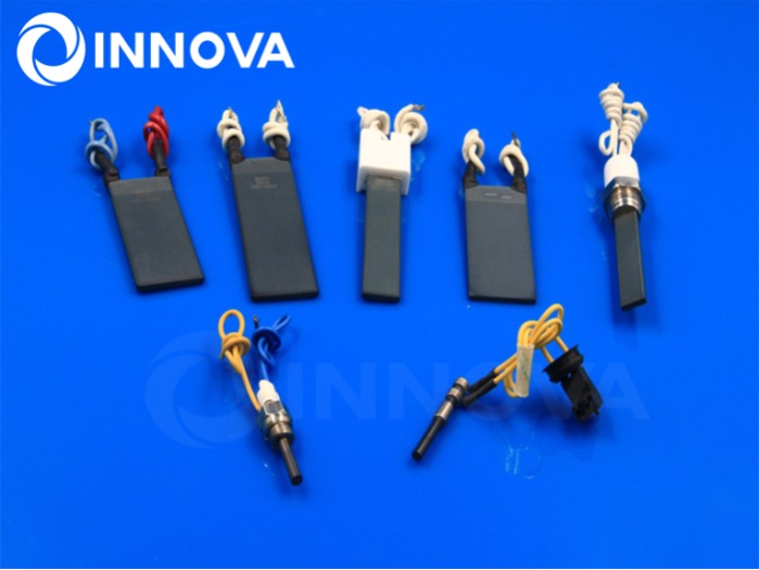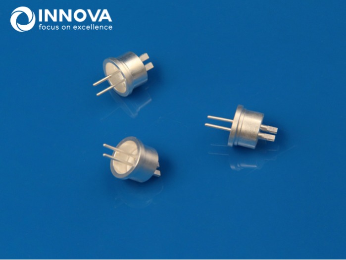
Multiple Connectors Explained: A Reliable Solution for Advan
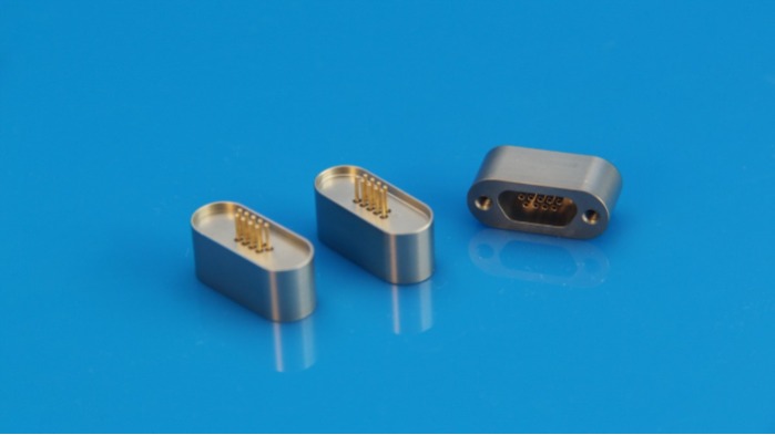
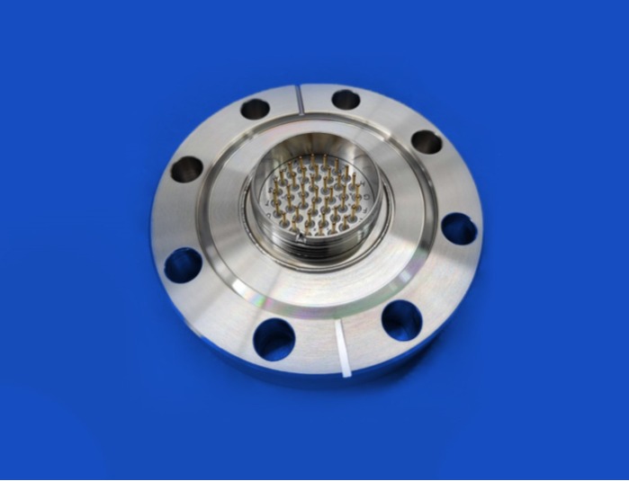
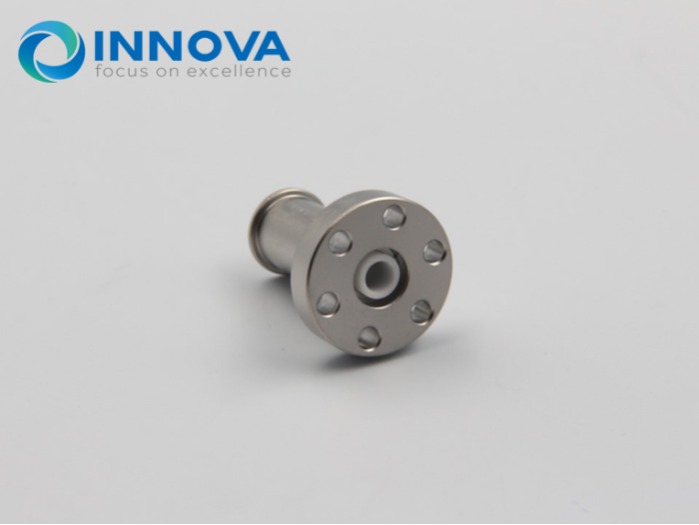
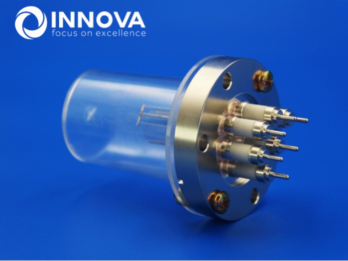
Ürün lansmanı ・ 5 Eyl 2024 ・ daha fazla…In the realm of advanced electronics, the demand for reliable, high-performance connectors has never been greater. Among the numerous options available, Multiple Connectors stand out for their versatility and robustness. These connectors play a critical role in ensuring stable and efficient connections in various high-tech industries, particularly in applications where Ceramic-to-Metal integration is crucial. Understanding Multiple Connectors Multiple Connectors are designed to accommodate several electrical connections within a single housing, making them ideal for complex systems where space and reliability are paramount. These connectors are often used in environments where harsh conditions, such as high temperatures and corrosive atmospheres, are present. Their ability to maintain a stable electrical connection, even under extreme conditions, makes them indispensable in industries like aerospace, defense, and medical devices.